ADC INTERFACING WITH ARM
The input to an analog-to-digital converter, (ADC) consists of a voltage that varies among a theoretically infinite number of values. It demonstrates the principle behind interfacing ADC with ARM LPC2148. A microcontroller, a digital device, can read, execute and transmit only digital signals.
Analog-to-digital conversion is an electronic process in which a continuously variable (analog) signal is changed without altering its essential content, into a multi-level (digital) signal. The input to an analog-to-digital converter, (ADC) consists of a voltage that varies among a theoretically infinite number of values. It demonstrates the principle behind interfacing ADC with ARM LPC2148. A microcontroller, a digital device, can read, execute and transmit only digital signals. On the contrary, the outputs of the most of the transducers, temperature, pressure, force are analog in nature which is coverted into electrical signals. Thus it is hard to interface these transducers directly with controllers.

Analog-to-digital convertor (ADC) ICs are one way make the analog input compatible with the microcontroller. It is an intermediate device to convert the signals from analog to digital form. These digital signals are used for further processing by the digital processors. Using an external ADC adds complexity to the circuit. To avoid this complexity, ARM LPC2148 Microcontrollers have in-built ADC module which reduces the cost and connections of the circuit.

Description

ARM is one of the major options available for embedded system developer. LPC2148 is the widely used IC from ARM-7 family. It is manufactured by Philips and it is pre-loaded with many inbuilt peripherals making it more efficient and a reliable option for the beginners as well as high end application developer.

ARM is a family of instruction set architectures for computer processors based on a reduced instruction set computing (RISC) architecture developed by British company ARM Holdings .A RISC-based computer design approach means ARM processors require significantly fewer transistors than typical processors in average computers. This approach reduces costs, heat and power use. These are desirable traits for light, portable, battery-powered devices including smartphones, laptops, tablet and notepad computers and other embedded systems. A simpler design facilitates more efficient multi-core CPUs and higher core counts at lower cost, providing higher processing power and improved energy efficiency for servers and supercomputers.


The ARM LPC2148 features are as follows:

1. Architecture: ARM v4T

2. Processor: ARM7-TDMI-S

3. Instructions: 32-bit ARM and 16-bit Thumb

4. Debug support: RT Embedded ICE, Embedded Trace interface

5. Static RAM: 32 KB

6. (On-chip)Additional: 8 KB for USB DMA

7. Flash Program: 512 KB

8. Mem.(On-chip)Programming: ISP/IAP via on-chip boot-loader program

9. GPIO No. of pins: up to 45 (fast GPIO lines, 5V tolerant), Configurable to fast GPIO

10. External Interrupts: Four; No. of pins: Nine

The ARM LPC2148 has two ports Port 0 and Port 1 respectively each port contains 32-bits for I/O operations. The Port 0 has 32-bit of I/O pins for individual directions and Port 1 has 32-bits of I/O pins for bidirectional purpose. It has two timers of each 32-bit. It has capable to storing 128-bit memory for interfacing.

Over the last few years, the ARM architecture has become the most pervasive 32-bitarchitecture in the world, with wide range of ICs available from various IC manufacturers. ARM processors are embedded in products ranging from cell/mobile phones to automotive braking systems. A worldwide community of ARM partners and third-party vendors has developed among semiconductor and product design companies, including hardware engineers, system designers, and software developers.

Analog to Digital Converter (ADC) is used to convert analog signal/voltage into its equivalent digital number so that microcontroller can process that numbers and make it human readable.


The ADC in LPC2148 ARM7 Microcontroller is 10-bit successive approximation analog to digital converter. The features are listed as:

The ADC in LPC2148 ARM7 Microcontroller is 10-bit successive approximation analog to digital converter. The features are listed as:

• LPC2148 has two inbuilt ADC Modules, named as ADC0 & ADC1.

• ADC0 has 6-Channels (AD0.1-AD0.6).

• ADC1 has 8-Channels (AD1.0-AD1.7).

• ADC operating frequency is 4.5 MHz (max.), operating frequency decides the conversion time.

• Supports power down mode.

• Burst conversion mode for single or multiple inputs.


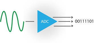
Registers of ADC in LPC2148 Microcontroller

There are several registers which will be used to setup and configure ADC feature in LPC2148. They are as follows:


1.  AD0CR (ADC0 Control Register)

• AD0CR is a 32-bit register.

• This register must be written to select the operating mode before A/D conversion can occur.

• It is used for selecting channel of ADC, clock frequency for ADC, number of clocks or number of bits in result, start of conversion and few other parameters.


Bits 7:0 – SEL

These bits select ADC0 channel as analog input. In software-controlled mode, only one of these bits should be 1.e.g. bit 7 (10000000) selects AD0.7 channel as analog input.

Bits 15:8 – CLKDIV

The APB(ARM Peripheral Bus)clock is divided by this value plus one, to produce the clock for ADC.

This clock should be less than or equal to 4.5MHz.

Bit 16 – BURST

0 = Conversions are software controlled and require 11 clocks

1 = In Burst mode ADC does repeated conversions at the rate selected by the CLKS field for the analog inputs selected by SEL field. It can be terminated by clearing this bit, but the conversion that is in progress will be completed.

When Burst = 1, the START bits must be 000, otherwise the conversions will not start.

Bits 19:17 – CLKS

Selects the number of clocks used for each conversion in burst mode and the number of bits of accuracy of Result bits of AD0DR.

e.g. 000 uses 11 clocks for each conversion and provide 10 bits of result in corresponding ADDR register.

000 = 11 clocks / 10 bits

001 = 10 clocks / 9 bits

010 = 9 clocks / 8 bits

011 = 8 clocks / 7 bits

100 = 7 clocks / 6 bits

101 = 6 clocks / 5 bits

110 = 5 clocks / 4 bits

111 = 4 clocks / 3 bits

• Bit 20 – RESERVED

Bit 26:24 – START

When BURST bit is 0, these bits control whether and when A/D conversion is started

000 = No start (Should be used when clearing PDN to 0)

001 = Start conversion now

010 = Start conversion when edge selected by bit 27 of this register occurs on CAP0.2/MAT0.2 pin

011= Start conversion when edge selected by bit 27 of this register occurs on CAP0.0/MAT0.0 pin

100 = Start conversion when edge selected by bit 27 of this register occurs on MAT0.1 pin

101 = Start conversion when edge selected by bit 27 of this register occurs on MAT0.3 pin

110 = Start conversion when edge selected by bit 27 of this register occurs on MAT1.0 pin

111 = Start conversion when edge selected by bit 27 of this register occurs on MAT1.1 pin

Bit 27 – EDGE

This bit is significant only when the Start field contains 010-111. In these cases,

0 = Start conversion on a rising edge on the selected CAP/MAT signal

1 = Start conversion on a falling edge on the selected CAP/MAT signal

• Bit 31:28 – RESERVED

2.  AD0GDR (ADC0 Global Data Register)

• AD0GDR is a 32-bit register.

• This register contains the ADC’s DONE bit and the result of the most recent A/D conversion.


• Bit 5:0 – RESERVED

Bits 15:6 – RESULT

When DONE bit is set to 1, this field contains 10-bit ADC result that has a value in the range of 0 (less than or equal to VSSA) to 1023 (greater than or equal to VREF).

• Bit 23:16 – RESERVED

Bits 26:24 – CHN

These bits contain the channel from which ADC value is read.

e.g. 000 identifies that the RESULT field contains ADC value of channel 0.

• Bit 29:27 – RESERVED

Bit 30 – Overrun

This bit is set to 1 in burst mode if the result of one or more conversions is lost and overwritten before the conversion that produced the result in the RESULT bits. This bit is cleared by reading this register.

Bit 31 – DONE

This bit is set to 1 when an A/D conversion completes. It is cleared when this register is read and when the AD0CR is written.

Bit 31 – DONE

This bit is set to 1 when an A/D conversion completes. It is cleared when this register is read and when the AD0CR is written.

If AD0CR is written while a conversion is still in progress, this bit is set and new conversion is started.

3.  ADGSR (A/D Global Start Register)

• ADGSR is a 32-bit register.

• Software can write to this register to simultaneously start conversions on both ADC.


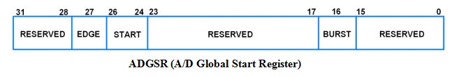
BURST (Bit 16), START (Bit <26:24>) & EDGE (Bit 27)

These bits have same function as in the individual ADC control registers i.e. AD0CR & AD1CR. Only difference is that we can use these function for both ADC commonly from this register.

  4.  AD0STAT (ADC0 Status Register)

• AD0STAT is a 32-bit register.

• It allows checking of status of all the A/D channels simultaneously.


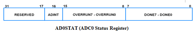
Bit 7:0 – DONE7:DONE0

These bits reflect the DONE status flag from the result registers for A/D channel 7 - channel 0.

Bit 15:8 – OVERRUN7:OVERRUN0

These bits reflect the OVERRUN status flag from the result registers for A/D channel 7 - channel 0.

Bit 16 – ADINT

This bit is 1 when any of the individual A/D channel DONE flags is asserted and enables ADC interrupt if any of interrupt is enabled in AD0INTEN register.

• Bit 31:17 – RESERVED

• Bit 31:17 – RESERVED

5.  AD0INTEN (ADC0 Interrupt Enable)
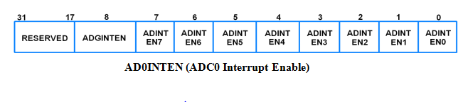
• AD0INTEN is a 32-bit register.

• It allows control over which channels generate an interrupt when conversion is completed.


Bit 0 – ADINTEN0

0 = Completion of a A/D conversion on ADC channel 0 will not generate an interrupt

1 = Completion of a conversion on ADC channel 0 will generate an interrupt

• Remaining ADINTEN bits have similar description as given for ADINTEN0.

Bit 8 – ADGINTEN

0 = Only the individual ADC channels enabled by ADINTEN7:0 will generate interrupts

1 = Only the global DONE flag in A/D Data Register is enabled to generate an interrupt

6.  AD0DR0-AD0DR7 (ADC0 Data Registers)
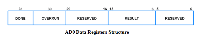
• These are 32-bit registers.

• They hold the result when A/D conversion is completed.

• They also include flags that indicate when a conversion has been completed and when a conversion overrun has occurred.


• Bit 5:0 – RESERVED

Bits 15:6 – RESULT

When DONE bit is set to 1, this field contains 10-bit ADC result that has a value in the range of 0 (less than or equal to VSSA) to 1023 (greater than or equal to VREF).

• Bit 29:16 – RESERVED

Bit 30 – Overrun

This bit is set to 1 in burst mode if the result of one or more conversions is lost and overwritten before the conversion that produced the result in the RESULT bits. This bit is cleared by reading this register.

Bit 31 – DONE

This bit is set to 1 when an A/D conversion completes. It is cleared when this register is read.

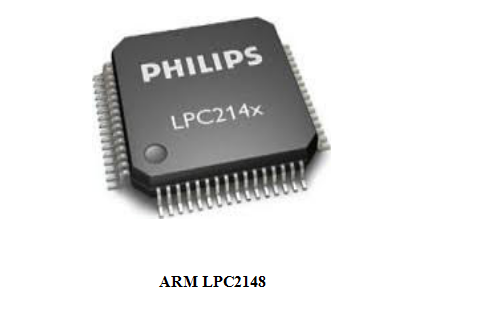
Programming Steps: ADC in LPC2148 ARM7 Microcontroller

• Configure input pin as analog input pin for ADC block

• Select channel we wish to use in our conversion

• Select clock for conversion & start conversion

• Wait for conversion to complete

• Read 10-bit conversion result

• Convert this result i.e. ADC output into decimal number

• Display reading on serial emulator or display device

Proteus design for ADC interfacing with ARM


Orcad design for ADC interfacing with ARM


ADC interfacing with ARM

/*  Name     : main.c
 *  Purpose  : Source code for ADC Interfacing with ARM LPC1248.
 *  Author   : Gemicates
 *  Date     : 2018-09-02
 *  Website  : www.gemicates.org
 *  Revision : None
 */
#include<lpc214x.h>                                                                 // header file for LPC21XX series
 
#define LCD (0xff<<16)                                                            
#define RS (1<<13)                                                                  // register select pin
#define RW (1<<14)                                                                  // read write pin
#define EN (1<<15)                                                                  // enable pin
 
void delay_fv(unsigned int x,int y);
 
void lcd_display(unsigned int x);
void cmd(unsigned char m);
void lcd_ini();
void lcd_pos(int line, int pos);
void lcd_str(unsigned char *x);
 
void adc_ini();
unsigned long int adc_data();
 
int main()
  {
		unsigned long temp;
		unsigned char first,second,third,fourth;
		PINSEL0=0X00000000;                                                 // select PORT0 as GPIO mode  
		IO0DIR=0XFFFFFFFF;                                                  // make PORT0 pin as Output mode 
		adc_ini();
		lcd_ini();
		lcd_str("TEMP VALUE IS");
		lcd_pos(2,6);
		lcd_display('C');
		while(1)                                                            // Repeat(loop) forever
	    {
					temp=adc_data();
					temp=temp*3300;
					temp=temp/1023;
					first=temp%10+'0';
					temp=temp/10;
					second=temp%10+'0';
					temp=temp/10;
					third=temp%10+'0';
					temp=temp/10;
					fourth=temp%10+'0';
					temp=temp/10;
					lcd_pos(2,0);
					lcd_display(fourth);
					lcd_display(third);
					lcd_display(second);
					lcd_display('.');
					lcd_display(first);
		
	    }
  }
 
void delay_fv(unsigned int x,int y)                                                 // Time delay function in milli seconds
  {
			 unsigned int i,j;
			 for(i=0;i<x;i++)
			 for(j=0;j<y;j++);
  }
void lcd_display(unsigned int x)                                                    // Function to send data to LCD
   {
			 IO0CLR|=(RS|RW|EN|LCD);
			 IO0SET|=(x<<16);
			 IO0SET|=RS;
			 IO0CLR|=RW;
			 IO0SET|=EN;
			 delay_fv(100,200);
			 IO0CLR|=EN;
			 delay_fv(10,10);
   }
 
void cmd(unsigned char m)                                                           // Function to send command to LCD
   {
			 IO0CLR|=(RS|RW|EN|LCD);
			 IO0SET|=(m<<16);
			 IO0CLR|=RS;
			 IO0CLR|=RW;
			 IO0SET|=EN;
			 delay_fv(100,10);
			 IO0CLR|=EN;
			 delay_fv(100,10);
   }
 
void lcd_ini()                                                                      // Funtion to Initialize LCD
  {
			cmd(0X38);                                                  // for using 8-bit 2 row mode and 5x7 Dots of LCD
			cmd(0X0C);                                                  // turn display ON for cursor OFF
			cmd(0X06);                                                  // display ON
			cmd(0X01);                                                  // clear screen
			cmd(0X80);                                                  // clear screen
  }
	
void lcd_pos(int line, int pos)                                                     // Function to select the position in LCD
  {                        
	    if(line==1)
		     cmd(0x80+pos);
	    else if(line==2)
		     cmd(0xc0+pos);
  }
	
void lcd_str(unsigned char *x)                                                      // Function to display in LCD
  {
	    while(*x!='\0')
	      {
		        lcd_display(*x);
		        x++;
	      }
  }


void adc_ini()
  {
		AD0CR = 1<<21;	                                                    // A/D is Operational
		AD0CR = 0<<21;	                                                    // A/D is in Power Down Mode
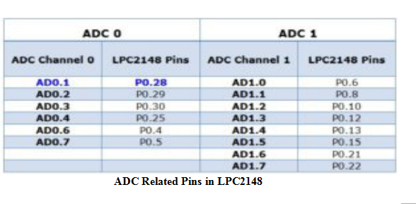
		PINSEL1 = 0x01000000;                                               // P0.28 is Configured as Analog to Digital Converter Pin AD0.1
		AD0CR = 0x00200802;                                                 // CLKDIV=4,Channel-0.1 Selected,BURST=0,EDGE=0
	
  }
	
unsigned long int adc_data()
   {
	      unsigned long rec;	
	      AD0CR |= (1<<24);					                    // Start Conversion
	      while(!(AD0GDR & 0x80000000));
/*Wait untill the DONE bits Sets*/
	      rec = AD0GDR;
	      AD0CR &= ~0x01000000;	                                            // Stops the A/D Conversion   				
	      rec = rec >> 6;                                                       // data is present after 6 bit
	      rec = rec & 0x3FF;                                                    // Clearing all other Bits
              return (rec);
   } 

Error message here!

Show Error message here!


Forgot your password?

Error message here!

Send OTP

Error message here!

Show Error message here!


Lost your password? Please enter your email address. You will receive a password you Need.

Send Error message here!


Back to log-in

Close